Component Design Approach and Layout Consideration of G-NAVPTM Topology
Abstract
In the design procedure, the component design and PCB layout greatly affect the performance of power supply. Careful PCB layout is critical to achieve low switching losses and clean, stable operation. Choosing appropriate component make the power supply easy passing the specifications of Intel and AMD. This application note will introduce the design approach of G-NAVPTM control topology, including on-time setting, switching frequency setting, load-line setting, and DCR current sensing network setting. After that, the recommend PCB layout rules will be showed to avoid noise interference to make the controller more robust.
1.Design Approach and Component Selection
The following design approach will use RT8884B as an example, which is designed to meet Intel VR12.5 specification. There are three main design procedures for RT8884B. The first step is initial settings for on-time and switching frequency. The second step is the DCR current sensing network design. Finally, we have to complete the load line design.
|
CPU Operation Condition
|
|
Input Voltage
|
12V
|
|
No. of Phases
|
3
|
|
VBOOT
|
1.7V
|
|
VDAC(MAX)
|
1.85V
|
|
ICCMAX
|
106A
|
|
ICC-DY
|
60A
|
|
ICC-TDC
|
55A
|
|
Load Line
|
1.5mΩ
|
|
Fast Slew Rate
|
12.5mΩ/μs
|
|
Max Switching Frequency
|
300kHz
|
Refer to Shark Bay VRTB power delivery guide, the recommended output filter is listed as follows :
Output Inductor : 360nH / 0.72mΩ
Output Bulk Capacitor : 560µF / 2.5V / 5mΩ (max) 4 to 5pcs
Output Ceramic Capacitor : 22µF / 0805 (18pcs max sites on top side)
1.1.Initial Setting for On-Time and Switching Frequency
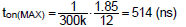
Generally, higher switching frequency can achieve faster transient response, smaller steady-state output ripple, and reduce power components' size and PCB space. However, the higher switching frequency will cause lower conversion efficiency, poor noise immunity and thermal issue. Therefore, the maximum switching frequency needs to be limited in a reasonable range to compromise between the pros and cons. After determining the maximum switching frequency, the maximum on-time can be obtained with the relation between the duty and switching frequency.

Where VDAC is the reference voltage, fsw,max is the maximum switching, and VIN(MAX) is the maximum input voltage. The following shows the design example of RT8884B.
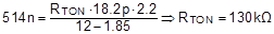
Since RT8884B is one kind of constant on-time control, the patented CCRCOT (Constant Current Ripple COT) technology can generate an adaptive on-time with input voltage and VID code to obtain a constant current ripple. So that the output voltage ripple can be controlled nearly like a constant at different input and output voltage operation range. Connect a resistor RTON between input voltage terminal and TONSET pin to set the on-time width.
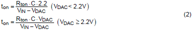
where C = 18.2pF
Where VIN is the maximum input voltage, VDAC is the reference voltage, and ton is the on-time which is determined in the above equation. The following shows the design example of RT8884B.
1.2.DCR Current Sensing Network Design
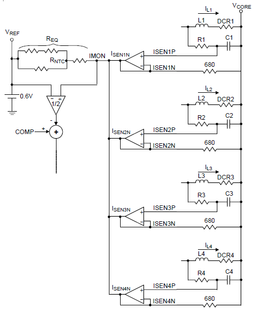
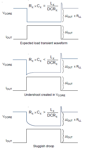
Figure 1. The whole current loop structure of RT8884B.
Figure 2. The corresponding output waveforms with different τCx and τLx time constant.
Figure 1 shows the whole current loop structure of RT8884B. The design of DCR current sensing network plays an important role in both ACLL performance and DCLL accuracy. For different time constant design, the ACLL behavior can be separated into three conditions as follows. Moreover, Figure 2 shows the corresponding output waveforms with different τCx and τLx time constant.
• If τCx matches τLx, an expected load transient waveform can be designed.
• If τCx is larger than τLx, output voltage has a sluggish droop as load increasing.
• If τCx is smaller than τLx, output voltage will sag to reduce the margin of undershoot specification.
Where DCRx is the equivalent resistance of the inductor, Lx is the inductance of the inductor, and Rx and Cx is the DCR current sensing network parameters.
Usually, the τCx time constant will be designed equal or slightly larger than the τLx time constant to prevent the overshoot and undershoot to have more margin to pass the specification. Notice that, the Cx may attenuate because of the bias voltage, temperature, or frequency…etc. As design the DCR current sensing network, the attenuate effect on the Cx is needed to be considered.
Since the copper wire of inductor has a positive temperature coefficient, DCR value is increased linearly with an increase of load current. Therefore, for achieving a better DCLL performance, a thermal compensation network with NTC thermister (REQ) is necessary to compensate the positive temperature coefficient of inductor DCR. The detailed thermal compensation can refer to design tool for specific product.
1.3.Load-Line Design
In the G-NAVPTM topology, the load line design depends on the ratio of current loop gain and voltage loop gain. The detailed load line equation will be shown in the corresponding IC datasheet. The following is using RT8884B as an example.
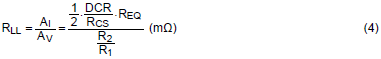
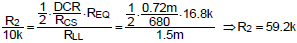
Where DCR (25°C) = 0.72mΩ, RCS = 680Ω is the current sensing resistor, REQ (25°C) is designed for the thermal compensation, and the R2 / R1 is the compensator AV gain. Through this equation, the load line can be changed simply by adjusting the compensator AV gain. Following Intel VR12.5 specification, a 1.5 (mW) load line is required; therefore, the R2 / R1 AV gain can be decided. The design example of RT8884B is shown as below.
2.Layout Consideration
Careful PC board layout is critical to achieve low switching losses and clean, stable operation. The switching power stage requires particular attention. If possible, mount all of the power components on the top side of the board with their ground terminals flushed against one another. Follow these guidelines for optimum PC board layout :
2.1.Power Stage Layout Guideline
• Keep the high current paths short, especially at the ground terminals.
• Keep the power traces and load connections short. This is essential for high efficiency.
• When trade-off between the charging path and the discharging path of the inductor, it's preferable to let the inductor charging path longer than the discharging path.
2.2.IC Sensing Pad and RGND Layout Guideline
•Place the current sense component (CX, RCSX, RX) close to the controller to avoid the current sensing signals be coupled by the noise.
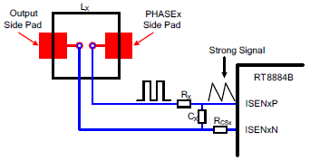
Figure 3. Placement of current sensing components.
• ISENxP and ISENxN connections for current limit and voltage positioning must be made using Kelvin sense connections to guarantee current sense accuracy. The traces from the inductor are run directly from the inductor pad and not from the connection plane of the inductor.
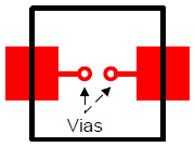
Figure 4. The inductor pad for current sensing traces.
• The PCB trace from the inductor sense nodes should be paralleled back to the controller. Typically these traces are run underneath the inductors on the bottom layer of PCB. If these traces run on an inner layer, there must be a ground plane above the current sense traces as a shielding from the top layer.
• Route high speed switching nodes (PWM, UG, LG, phase, etc…) away from sensitive analog areas (COMP, FB, ISENxP, ISENxN, etc...).
• Users need to connect exposed pad to the ground plane through low impedance path. The use of at least 5 vias to connect to ground planes in PCB internal layers is recommended.
3.Experimental Result and Conclusion
3.1.Experimental Result
Figure 5 shows the RT8884B EVB sample, which is applied in VR12.5 applications and can supports 4/3/2/1 phase. The measured load line curve and efficiency is showed in Figure 6. From the measured result, the G-NAVPTM topology can provide an accurate load line and still maintain the higher efficiency. Figure 7 shows a large step and a small step load transient waveform, which indicates fast and stable transient performance and proper AVP control.
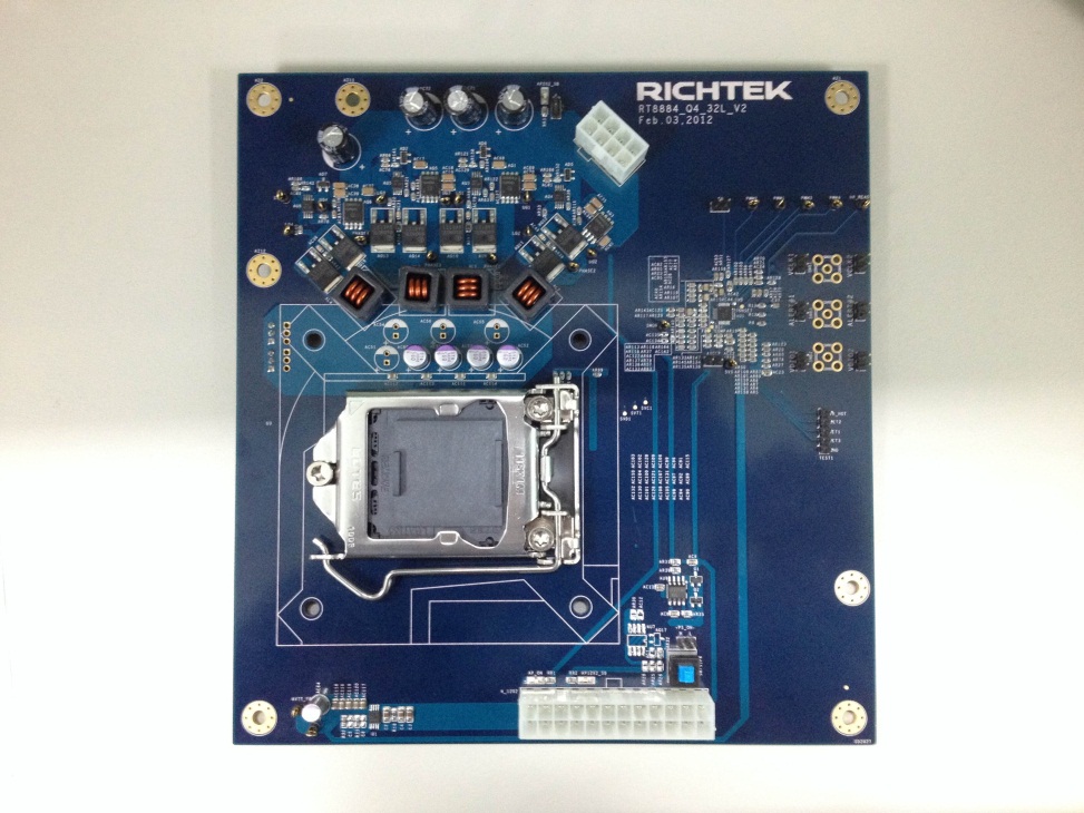
Figure 5. The EVB sample of RT8884B.
Table 1. EVB testing condition
|
VIN
|
12V
|
|
VOUT
|
1.8V @PS0
|
|
Phase Number
|
4
|
|
Ls
|
360nH / 0.72mΩ
|
|
Co
|
OSCON : 470µF / 4.5mΩ*4
MLCC : 22µF*19
|
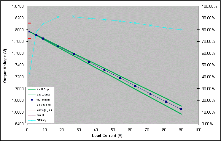
Figure 6. Measured load-line and efficiency from RT8884B.
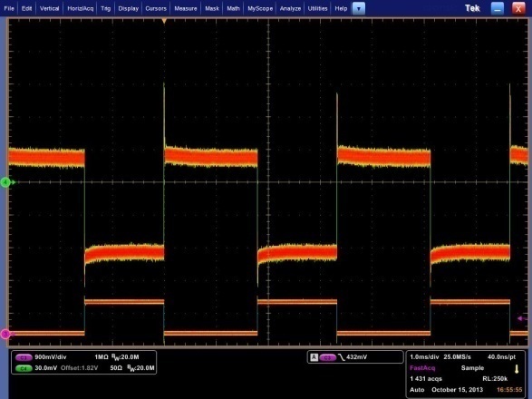
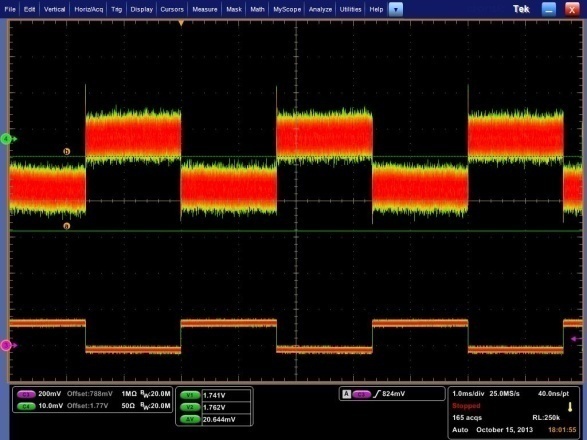
(CH3: Loading current (900mv/Div) ; CH4: Output voltage (30mV/Div))
(a) Large step (1A-61A) ACLL @300Hz (b) Small step (50A-60A) ACLL @300Hz
Figure 7. Measured ACLL result from RT8884B.
3.2.Conclusion
The design of the system components usually needs to compromise between lots of restrictions to gain the most benefit on the efficiency and performance. Besides, the particular layout skills are used to minimize the effect of the parasitic component and avoid the high speed switching noise coupling. This application note shows the general design approach of G-NAVPTM control topology and the PCB layout rules. Following the rules mentioned above, users can use Richtek’s controller IC without any inconvenience.
4.Reference
[1] Richtek, RT8884B datasheet.
[2] Intel document, “Shark Bay Ultrabook™ Platform Power Delivery”
[3] Intel document, “Shark Bay Mobile Platform Power Delivery”
[4] Intel document, “Shark Bay Desktop and Denlow-WS Platform”